
Page 83 - Annual Report_21-22
P. 83
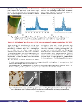
The  colour  during  dye  degradation  can  be  monitored   has been used as a programming language to write the
            using  Colour  Sensor.  This  sensor usually  detects colour   programs. The below figure represents the spectrum of
            in RGB (red, green and blue) scale. The colour sensor has   Eosin Yellowish obtained from the spectrograph and the
            been designed using both hardware and software. Python   predicted spectrum of Eosin Yellowish.


            (a)                   (b)                                        (c)
                  Fig 4. (a) The image of Eosin Yellowish, (b) the spectrum of Eosin Yellowish obtained from
                               spectrograph and (c) the predicted spectrum of Eosin Yellowish are presented

             Synthesis of Mo-based Two-dimensional (2D) heterostructures for device applications (OLP-104)

            Two-dimensional  (2D)  layered  materials  such  as  metal   stoichiometric state with  various  hetero-interfaces
            chalcogenides  (MCs)  have  been  studied  extensively  for   and  determine their exact atomic-scale structures to
            optoelectronic applications due to their sizeable bandgap   understand their structure-property correlation. Our long-
            in  the visible  and  near-infrared range,  mechanical   term goal is to fabricate various 2D metal chalcogenides
            flexibility,  strong  light-matter  interaction  at  monolayer   material and their heterointerfaces on other 2D layered
            thickness. Optoelectronic devices such as photodetectors,   substrates  using  chemical  vapour  deposition  (CVD)  and
            photovoltaics  (PV)  and  light-emitting  devices  have  been   perform  atomic-scale  interfacial  studies  of  multilayered
            demonstrated using MCs of various device architectures   structures to get the highly efficient and flexible module
            and measurements.                                 for device applications. The following work has been done.
            Thus, it is essential to fabricate these materials at their
            •  Three independent temperature gradient zone chemical vapour deposition(CVD) equipment is successfully customized
                and installed for the growth of various 2D materials.
            •  MoO  2d materials of various thicknesses are successfully synthesized using the CVD method. (as shown in figure 1).
                  3
            •  The Structural study has been performed using the newly installed JEOL JEM-F200 TEM at IMMT.


               Figure 1: (a) Optical microscopy (b) SEM image of CVD-grown 2D MoO  flakes (c) selected area electron diffraction
                                                                       3
                 (SAED) of the flakes and (d) corresponding HRTEM image and crystal structure (inset) shows the presence of
                                                     α- MoO  structures.
                                                           3


            ANNUAL REPORT 2021-22                                                                               81